The complete guide to PCB pad :types, size, spacing, repair and comparison - IBE Electronics

Soldering is one of the most important processes in PCBA processing. On printed circuit boards, electrical connections to all components are made via PCB pads. The PCB pads are a very critical part of the PCB that determines where components are soldered on the PCB.The size, shape, and position of pads in a PCB directly depend on the manufacturing quality of the board. Today we will take a look at the PCB pad in SMT soldering.
Soldering is one of the most important processes in PCBA processing. On printed circuit boards, electrical connections to all components are made via PCB pad.
PCB Soldering Techniques What Soldering Equipment You Need
Demystifying PCB Transformers – A Complete Guide - Mainpcba One-stop PCB Assembly Manufacturer

What is a Pad in PCB Design? - JHYPCB
PCB Buyer's Guide
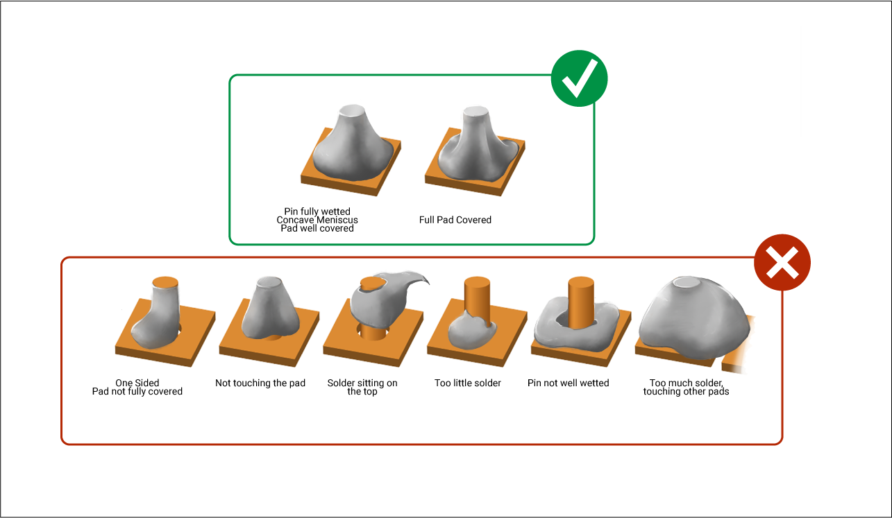
IPC J-STD-001 Standard for Soldering
Best Methods for Calculating SMD Pad Size in PCB Design
The Ultimate Guide to PCBA: Process, Types, and Techniques for the Electronics Enthusiast
Types of PCB Connectors: An In-Depth Guide

The complete guide to PCB pad :types, size, spacing, repair and comparison - IBE Electronics

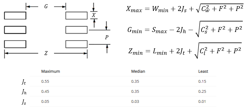
PCB Pad Size Guidelines: Finding the Proper Pad Sizes for Your Circuit Design
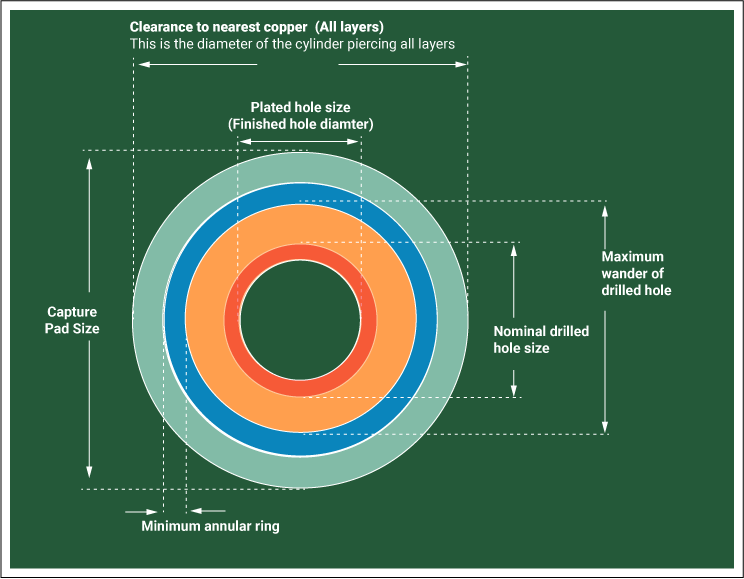
What is a Pad in PCB Design and Development
PCB Pad Size Guidelines: Finding the Proper Pad Sizes for Your Circuit Design